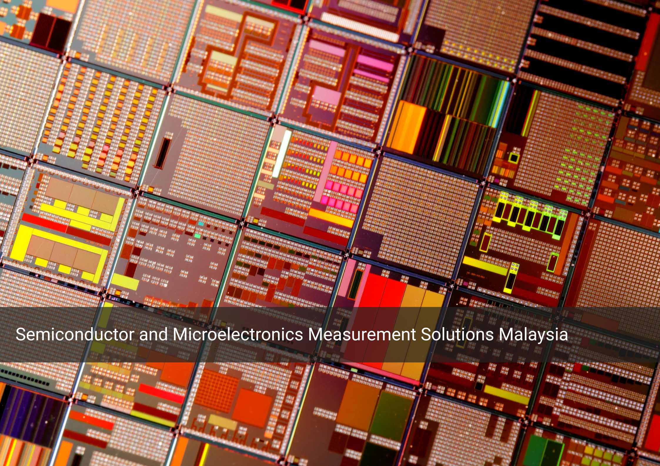
Semiconductor manufacturing operates at micron and sub-micron precision levels. As chip designs become smaller and more complex, dimensional control and defect detection become increasingly critical.
Advanced electronics measurement solutions Malaysia enable semiconductor manufacturers to maintain high accuracy throughout wafer fabrication, chip packaging, and microelectronics assembly processes.
Micron-Level Accuracy in Wafer Fabrication
Wafer fabrication involves highly sensitive processes such as photolithography, etching, and deposition. Even minimal deviations can affect electrical performance and product reliability.
To ensure structural consistency, manufacturers implement:
Wafer thickness measurement
Surface profile analysis
Pattern alignment verification
Micro-defect detection
High-resolution optical systems are commonly used in these environments due to their non-contact and precision capabilities.
Providers such as Hansvue support industrial inspection environments with advanced imaging and optical measurement technologies suitable for delicate semiconductor components.
Non-Contact Optical Measurement Technologies
Because semiconductor components are extremely fragile, physical contact measurement methods are often avoided.
Modern electronics measurement solutions Malaysia may include:
Optical microscopy systems
3D surface profiling
Laser scanning technologies
Automated defect recognition systems
These technologies improve inspection reliability while minimizing contamination or mechanical interference.
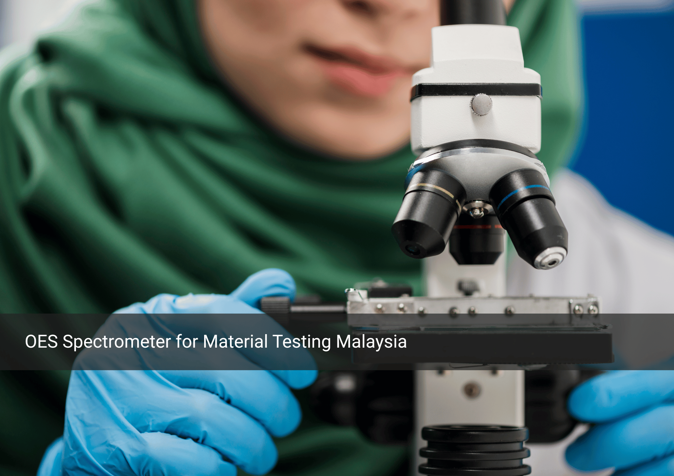
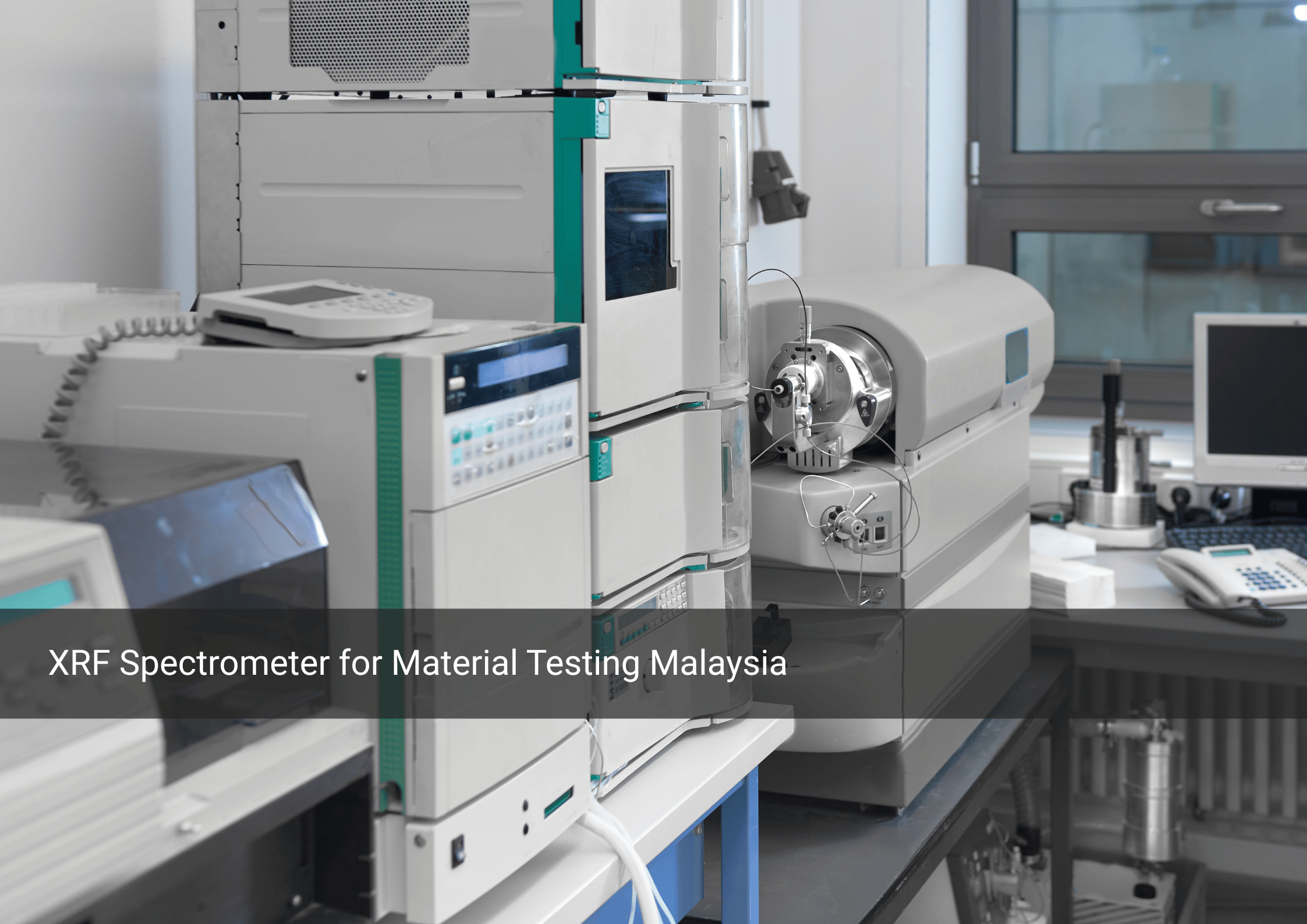
Laboratory Validation and Analytical Support
Beyond dimensional inspection, semiconductor manufacturing may require laboratory-based validation to verify material integrity and composition.
Analytical instrumentation used in controlled lab environments helps support:
Material characterization
Surface analysis
Failure investigation
Research and development testing
Organizations such as JS Analytical contribute laboratory and analytical equipment that supports advanced industrial verification processes where deeper material validation is required.
Improving Yield and Production Stability
In semiconductor manufacturing, yield rate directly impacts profitability. Accurate measurement systems help manufacturers:
Detect micro defects early
Reduce wafer rejection
Stabilize process parameters
Improve repeatability
Strong implementation of electronics measurement solutions Malaysia reduces production loss and strengthens overall manufacturing efficiency.
Conclusion
Semiconductor and microelectronics production require precision at the highest level of modern manufacturing. By integrating advanced optical systems, laboratory validation tools, and automated inspection technologies, manufacturers can maintain strict quality control and improve yield performance.
With the right electronics measurement solutions Malaysia, companies can support innovation while maintaining reliability in highly competitive global markets.