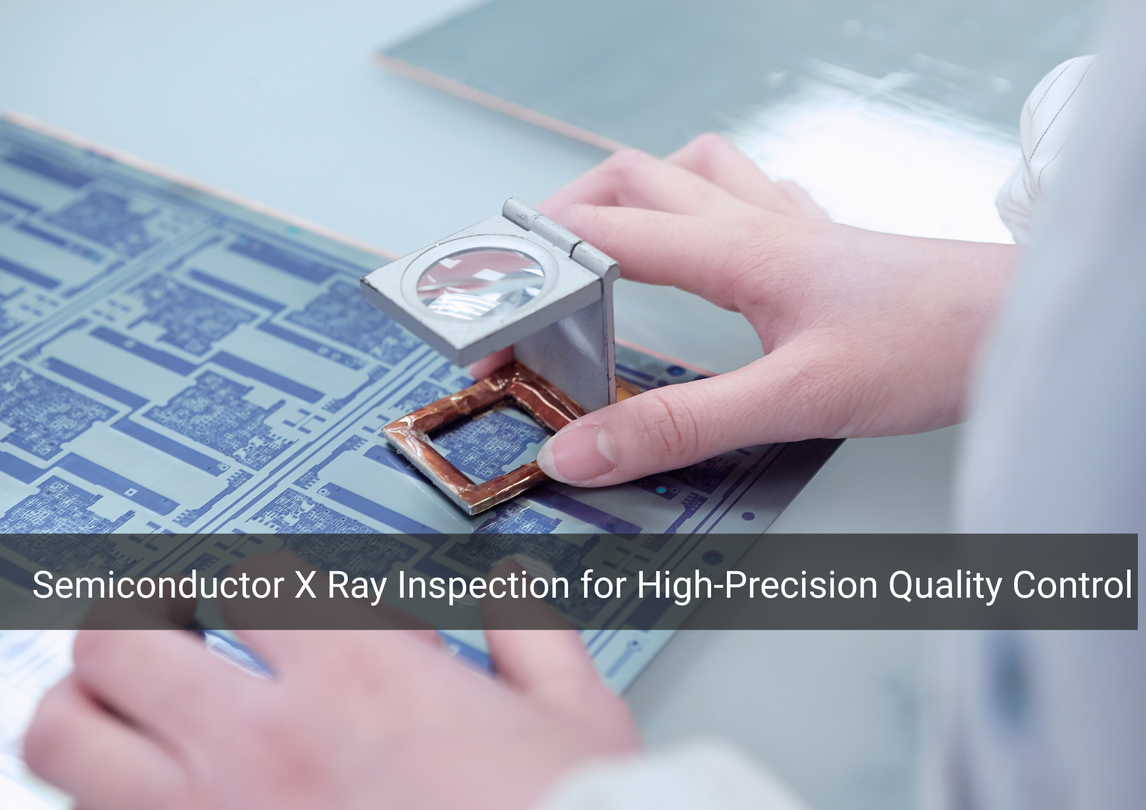
The semiconductor industry demands extreme precision. As electronic devices become smaller and more powerful, internal structures within chips and packages grow increasingly complex. Detecting defects without damaging sensitive components is a major challenge. This is where Semiconductor X Ray Inspection becomes essential.
Unlike surface-level inspection methods, X-ray technology allows manufacturers to see inside semiconductor packages, solder joints, and internal connections without physical disassembly. This ensures product reliability while maintaining high production efficiency.
Why Semiconductor X Ray Inspection Is Critical
Semiconductor components often contain hidden solder joints, ball grid arrays (BGA), microvias, and internal wiring that cannot be visually inspected. Even minor voids or cracks can lead to device failure.
Semiconductor X Ray Inspection helps detect:
Solder joint voids
Internal cracks
Misalignment in BGA components
Wire bond defects
Voids in encapsulated chips
By identifying these defects early, manufacturers can prevent costly recalls and maintain strict quality standards.
How X Ray Inspection Technology Works
Semiconductor X Ray Inspection systems generate controlled X-ray beams that pass through the component. Differences in material density create contrast in the captured image, allowing operators to identify structural irregularities.
Advanced systems offer:
High-resolution imaging
2D and 3D (CT) inspection capabilities
Automated defect recognition
Digital image analysis and reporting
Companies looking for reliable inspection systems often consider solutions from Hansvue, known for providing precision measurement and inspection technologies suited for industrial applications.
Supporting Semiconductor Manufacturing Ecosystem
Inspection is only one part of semiconductor quality assurance. Laboratory validation and calibration services from companies such as Obsnap and JS Analytikal help ensure inspection equipment performs consistently and meets compliance requirements.
Additionally, materials used in semiconductor packaging must meet strict standards. Suppliers like Victor Material contribute by providing high-quality engineered materials that support structural reliability before inspection even begins.
By integrating material quality, laboratory validation, and Semiconductor X Ray Inspection, manufacturers build a complete and reliable production ecosystem.
Benefits for Reliability and Compliance
Implementing Semiconductor X Ray Inspection provides several advantages:
Early defect detection
Improved product reliability
Reduced rework and scrap rates
Compliance with international electronics standards
Enhanced traceability through digital reporting
As semiconductor devices are used in automotive, medical, and aerospace industries, reliability becomes even more critical.
Conclusion
Semiconductor X Ray Inspection is an essential technology for ensuring product integrity in advanced electronics manufacturing. By detecting hidden internal defects without damaging components, manufacturers can maintain high reliability and industry compliance.
With advanced inspection solutions from Hansvue and complementary support from laboratory and material specialists such as Obsnap, JS Analytical, and Victor Material, semiconductor manufacturers can confidently meet evolving technological demands.